Scanning Tunneling Potentiometry
Two-dimensional (2D) material systems and heterostructures have recently emerged as a promising class of materials allowing to address a variety of functionalities, including field-effect modulation of electronic and magnetic properties, different regimes of electron and spin transport, as well as spin current generation and manipulation. Present investigations of charge and spin transport phenomena in novel material systems are widely based on lithographically defined devices. Although, these measurements provide valuable understanding of different spin and charge transport processes, a fixed device geometry inherently lacks spatial resolution and microscopic insights into local structure and morphology dependent properties. However, such local investigations are important for a deeper understanding of material-related phenomena, in particular for van der Waals heterostructures of 2D materials where interfaces and defects play a crucial role.
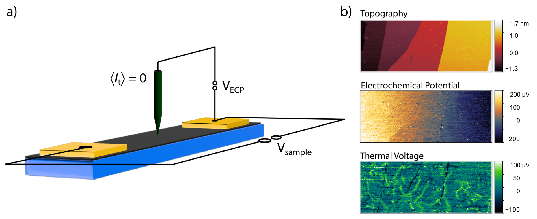
In recent years, several investigations of local electronic and spin transport phenomena emerged involving different techniques. The flow of electrons in graphene was studied using a single-electron transistor, SQUID or a nitrogen-vacancy defect (NV center) placed at the tip of an atomic force microscope (AFM). In this way, local electrostatic and magnetic fields, as given by the current distribution, can be sensed, thereby allowing to draw conclusions on the current density in homogeneous materials. These methods achieve a resolution of micrometer down to a few tens of nanometers but are not able to observe atomistic variations of the electronic states and atomistic structural features of the electrical transport channels. A different and complementary technique is scanning tunneling potentiometry (STP), see Fig. 1a. It is based on scanning tunneling microscopy (STM), which measures a tiny tunneling current with high precision between a biased substrate with respect to a sharp metallic tip. Thereby, STM provides information on the atomic and electronic structure of the surface of a conductive material with sub-Angstrom resolution. In STP mode, the local electrochemical potential can be measured with a compensation technique by applying a potential to a current-biased device such that the tunneling current between tip of the STM and the substrate vanishes. The compensation voltage is then equal to the local electrochemical potential and so-called thermal voltage, which can be disentangled measured with µV sensitivity simultaneously with atomically resolved topographic features of the sample (Fig. 1b). In recent years, STP has been applied to measure the local resistivities of metallic thin films, topological insulators and also graphene providing insights into variations of the electrical conductivity across crystalline steps and domain boundaries.
In our laboratory, we have recently implemented STP as a fully digital procedure into our variable temperature STM achieving very low noise levels [1]. We further analyzed the total noise contributions to the STP signal and tested different implementations. Applying this methodology to bare and Li intercalated graphene sheets grown on SiC, we followed the Li intercalation in the monolayer and bilayer graphene sheets and measured the change in sheet resistance for the different phases [2]. In our research we aim to further develop the STP technique and apply it to model systems to understand local transport phenomena that arises between the different transport regimes of ballistic, diffusive and viscous electron flows and due to unusual electronic phases of matter. Direct imaging of the local electrochemical potential in nanodevices will provide insight into the intrinsic and extrinsic influences of material interfaces and local disorder at previously inaccessible length scales, shedding light on outstanding questions concerning the extent and locality of the proximity effects in complex 2D materials and their local electronic transport properties.
Selected publications
- Performance analysis and implementation of a scanning tunneling potentiometry setup: Toward low-noise and high-sensitivity measurements of the electrochemical potential, T. Markovic, W. Huang, P. Gambardella, and S. Stepanow, Review of Scientific Instruments, 92, 103707 (2021).
- Observation of different Li intercalation states and local doping in epitaxial mono- and bilayer graphene on SiC(0001), W. Huang, J. Seo, M. P. Canvan, P. Gambardella, and S. Stepanow, Nanoscale, 16, 3160 (2024).